KIMTIGO's memory storage device production procedure is meticulous and thorough. It begins with the use of the original Nano Flash package, designed to meet industrial-grade environment and usage requirements. The process includes high-temperature welding, printing, and surface mounting. Sub-board cutting and system testing ensure optimal functionality. The devices undergo rigorous testing, including high-temperature tests, constant temperature and humidity tests, and high-temperature aging tests. The final steps involve appearance comparison, detection, and sampling of DRAM and FLASH testing. The memory storage solutions are then ready for industrial packaging, ensuring they are safe and secure for distribution.
 Game On! How PCIe Gen3x4 SSDs Enhance Gaming PerformanceOctober 16, 2023Gaming has evolved leaps and bounds over the years, and today's gamers demand not only immersive graphics and responsive controls but also lightning-fast load times and minimal lag. Enter PCIe Gen...viewA Guide to Choosing the Perfect 1TB PCIe NVMe SSD for Your PCMarch 15, 2024Upgrading your PC's storage to a 1TB PCIe NVMe SSD can be a game-changing experience. With lightning-fast speeds and ample capacity, these SSDs are perfect for gamers, creative professionals, and anyo...view
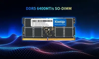 Kimtigo Overclocked DDR5 SODIMM Memory Makes a Strong Debut, Can be Stably Overclocked to 6400MT/sNovember 8, 2023Kimtigo is constantly pursuing innovation and breakthroughs in the field of storage, and is committed to improving product performance, efficiency and user experience. on September 6, Kimtigo's ne...view
 Size Doesn't Matter: Why a 2.5-Inch Solid State Drive Can Revolutionize Your Data StorageAugust 14, 2023In the world of technology, big changes often come in small packages. The 2.5-inch Solid State Drive (SSD) is a prime example of this concept. Despite its compact size, this storage device has the pot...view
 Unlocking Performance and Capacity: Discovering the Power of a 2.5-Inch SSD with 2TB CapacityAugust 15, 2023In the realm of modern computing, where data reigns supreme, the dynamic duo of performance and capacity has become the ultimate aspiration. Enter the 2.5-inch SSD with a staggering 2TB (terabytes) of...view
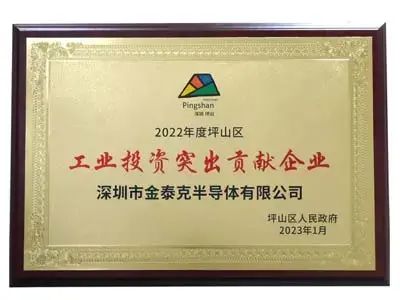 Kimtigo Won the Enterprise with Outstanding Contribution to Industrial Investment AwardMarch 22, 2023On February 6, 2023, the Pingshan District Entrepreneurs' Spring Symposium was held at the Pingshan Swallow Lake International Convention and Exhibition Center.Yang Jun, secretary of the Pingshan ...view
 EN
EN  es
es  ru
ru 


